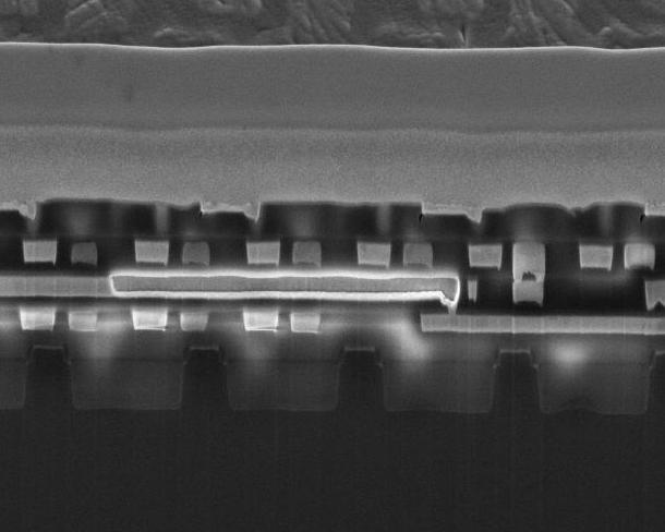
In the modern circuit, the reliability of the Cu interconnect/low-k dielectric system becomes one of the major factors to consider when it comes to the manufacturing of the device. The various issues on the reliability of the Cu interconnect/low-k dielectric system are EM (Electromigration) and TDDB (Time Dependent Dielectric Breakdown). In both cases, the failures happen over time. Thus predicting the lifetimes and modeling the failure mechanisms are important from the reliability study point of view. A part of this project studies the electromigration reliability of Cu interconnect under pulsed current conditions, which corresponds to most electrical signals in an integrated circuit. Samples fabricated using the latest technology nodes (45 nm and 90 nm CMOS) are being tested and characterized through wafer-level and package-level accelerated testing. The failed samples undergo failure analysis using FIB (Focus Ion Beam) cross-sectioning and TEM (Transmission Electron Microscope) imaging.
Our work on unipolar and bipolar pulsed current shows that Cu/low-k interconnects exhibit longer electromigration lifetime when the pulsed current have shorter half-period than the median-time-to-failure (t50) of direct current (D.C.) stressed samples. We observed that Cu/low-k interconnects exhibit characteristics of the On-Time model under unipolar pulsed current stress. The electromigration lifetime and failure site of Cu/low-k interconnects under bipolar pulsed current stress were found to depend on the via-to-interconnect structure and the direction of current flow in the first half-period. The overall goal is to improve the understanding on the circuit reliability of interconnects.
 |
 |
| Void formed at the dielectric cap/Cu interface after 760 hr of bipolar pulsed current electromigration test (1 hr pulse width, 50% duty cycle). | Void spanning 4.58 µm in length is observed after 260 hr of D.C. electromigration test. |
Similarly, the objective of the low-k dielectric reliability study is to improve the understanding of the actual failure mechanisms of Cu/low-k dielectric system in devices. This involves 3 areas: (1) to design and fabricate new test structures that are more representative of the actual layout, as well as allowing precise pin-pointing of the failure site by confining it to an area, (ii) to use pulsed voltage stress tests that reflect the non-DC signal propagations, and (iii) to study the different materials and process variations impact on the reliability of the system.
 |
| Examples of different failure mechanisms in low-k dielectrics |
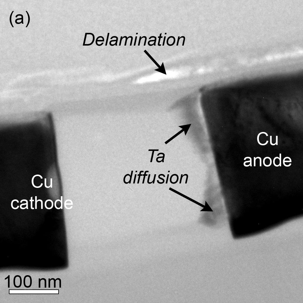
A three dimensional (3D) architecture at first glance seems to be an obvious answer to the interconnect delay problem and heterogeneous integration. The basic idea is to create multiple active layers which will reduce the total chip area, shortening critical interconnect lengths and reducing their power consumptions and delays. The 3D architecture also can be used to build stacked chips by placing different devices onto different layers. Since they are built on different layers, potential electromagnetic interference between such devices can be reduced. By fabricating such different technologies on separate substrates followed by physical bonding, it can reduce the integration complexity significantly. Many different technologies of IC-stacking are currently being developed by different groups around the world. The main difference between the various technologies is how the wafers/ICs are bonded.
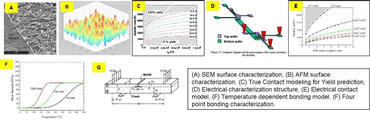
Direct Cu bonding in 3D-IC stacking has the advantage that Cu acts as both the bonding material and interconnect material. Understanding the fundamental mechanism in Cu thermocompression bonding is essential for bonding optimization. In this project, fundamental study of Cu thermocompression bonding is conducted. Relation of bonding parameters, such as surface properties to mechanical properties of Cu bonding is investigated. As a result, a model of bond integrity as a function of bonding parameters can be developed. Furthermore, a contact resistance model has also been developed, which is correlated with the bond strength so enable the non-destructive measurement of the bond strength.
 |
Separately,
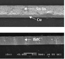
Sn-In material is investigated as a candidate for Low
Temperature Bonding Applications such as in MEMS devices.
Its melting point at eutectic composition which is 120oC,
is an interesting feature that enables bonding formation
at low temperature. Its ability to form Intermetallic
Compound (IMC) with Cu is also promising as it improves
the reliability of the bonding because IMC is known to
have high melting point.
In this project, the effects of bonding parameters such
as bonding pressure, temperature and time to the
microstructure and mechanical strength are studied.
In order to develop a non-destructive test, the
mechanical strength (Four Point Bend Test) is also
correlated with the contact resistance (Four Point Probe)
experimentally. Lastly, the effects of Sn-In composition
on the bonding ability to Cu are also investigated.
 |
 |
|
| a) | b) |
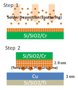
a) Experimental Procedure.
Step 1 : Solder Deposition by Sputter Deposition,
Step 2 : Bonding of Solder with Cu.
b) Cross Sectional View of Bonding Interface,
i) Bonded at 80oC Temperature, ii) Bonded at
200oC temperature
 |
|
| a) | b) |
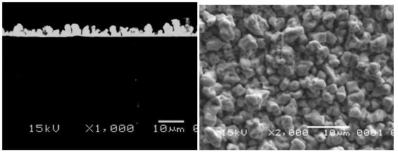
SEM Images of as-deposited 75Sn25In : a) Cross-sectional view and b) top view
| Nanowires
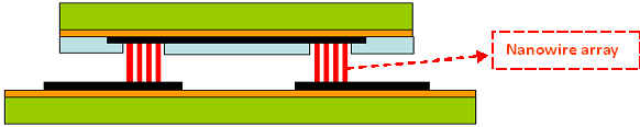
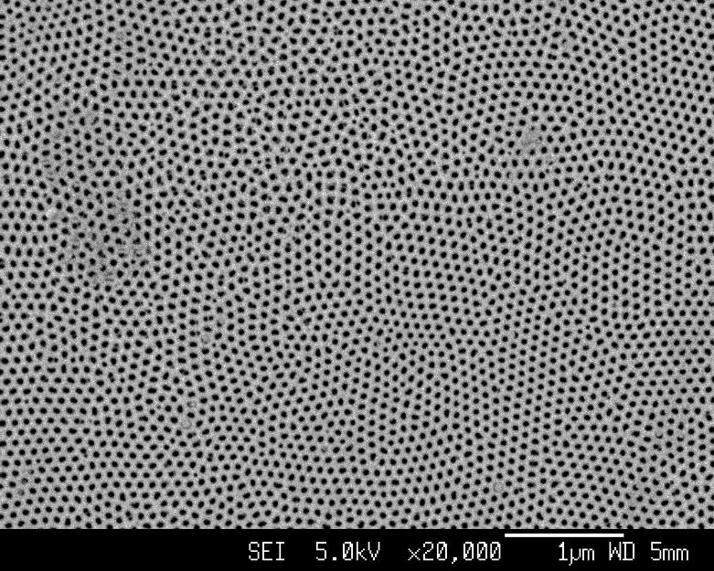
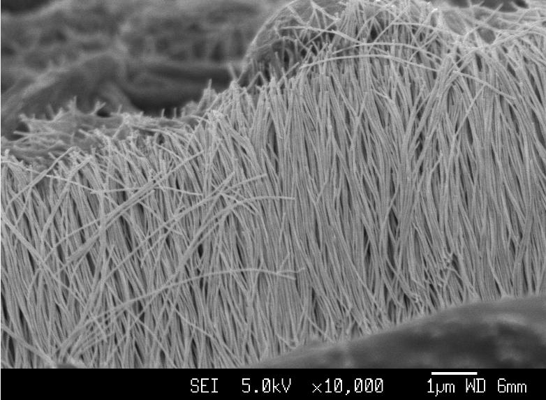
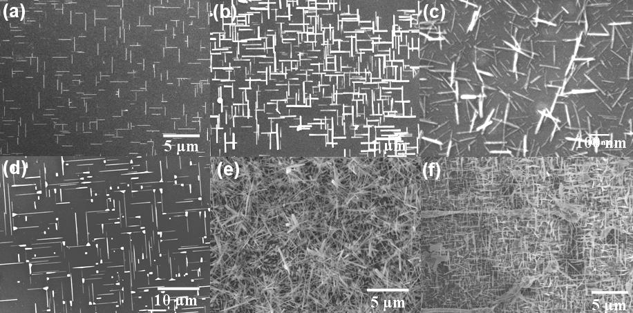
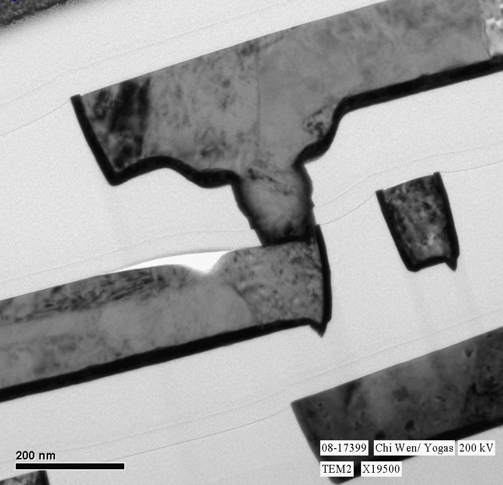
Interconnect Technology <back to top> Nanowires are one-dimensional nanostructures that have attracted considerable attention in recent years due to their novel physical properties and potential applications as interconnects in future generations of nanoelectronics. Due to CMOS scaling, off-chip interconnects needs to be kept in pace so as to match the device performance. International Technology Roadmap for Semiconductors (ITRS) has projected a solder bump pitch for flip chip to be below 20 µm by 2010. As pitch is decreasing, it poses a problem for the scalability and reliability of flip chip solder bump. As such, micro pads of metallic nanowire array is believed to be a viable alternative for fabricating fine pitch chip-to-substrate interconnects (Fig. 1). In addition, the use of in-situ fabricated nanowire array will have higher redundancy to fail compared to conventional single column interconnects. Due to its favourable characteristics such as tunable nanopore diameter, good mechanical strength and attainable uniform pore structure with hexagonally arrangement, Anodized Aluminum Oxide (AAO) templates (Fig. 2) are selected to deposit the metallic nanowires. Electrodeposition is then carried out to fill metallic nanowires (Fig. 3) into the nanoporous AAO template. The nanowire electrical properties are characterized, such as the resistivity and maximum failure current density. Current research also involves the reliability study and failure analysis of the nanowires due to electromigration.
A related investigation is on the synthesis on silicide nanowires. The reaction between SiO2 and Na2O has been intensively studied for one century by glass industry. We find a new synthesis route to fabricate single-crystalline silicide nanowires with controllable morphologies by manipulating this reaction. Catalyst and silica shell free silicide nanowires that were epitaxially aligned or free-standing were grown on silicon wafers under different growth conditions. The electrical properties of silicide nanowires were characterized and the results show that they are very attractive nanoscale building blocks for interconnects and fully silicided (FUSI) gate applications in nanoelectronics.
|
|||||||||||||