T. Tang and X. Zhou
School of Electrical and Electronic Engineering, Nanyang Technological
University
Nanyang Avenue, Singapore 639798, Republic of Singapore
Email: exzhou@ntuix.ntu.ac.sg
Abstract | Figures | Reprint | Back
(Click on the Figure inside the Paper to see its enlargement.)


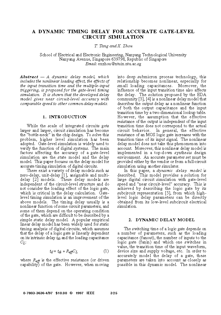
Fig. 1 Schematic of the test circuit.
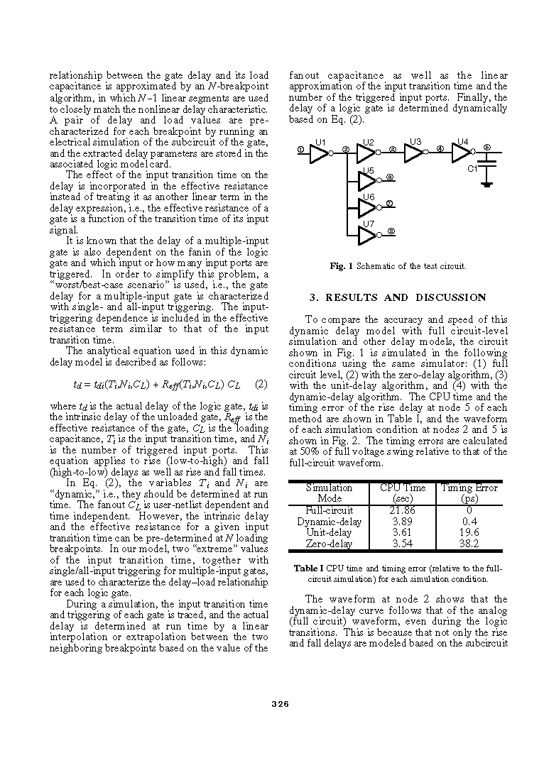
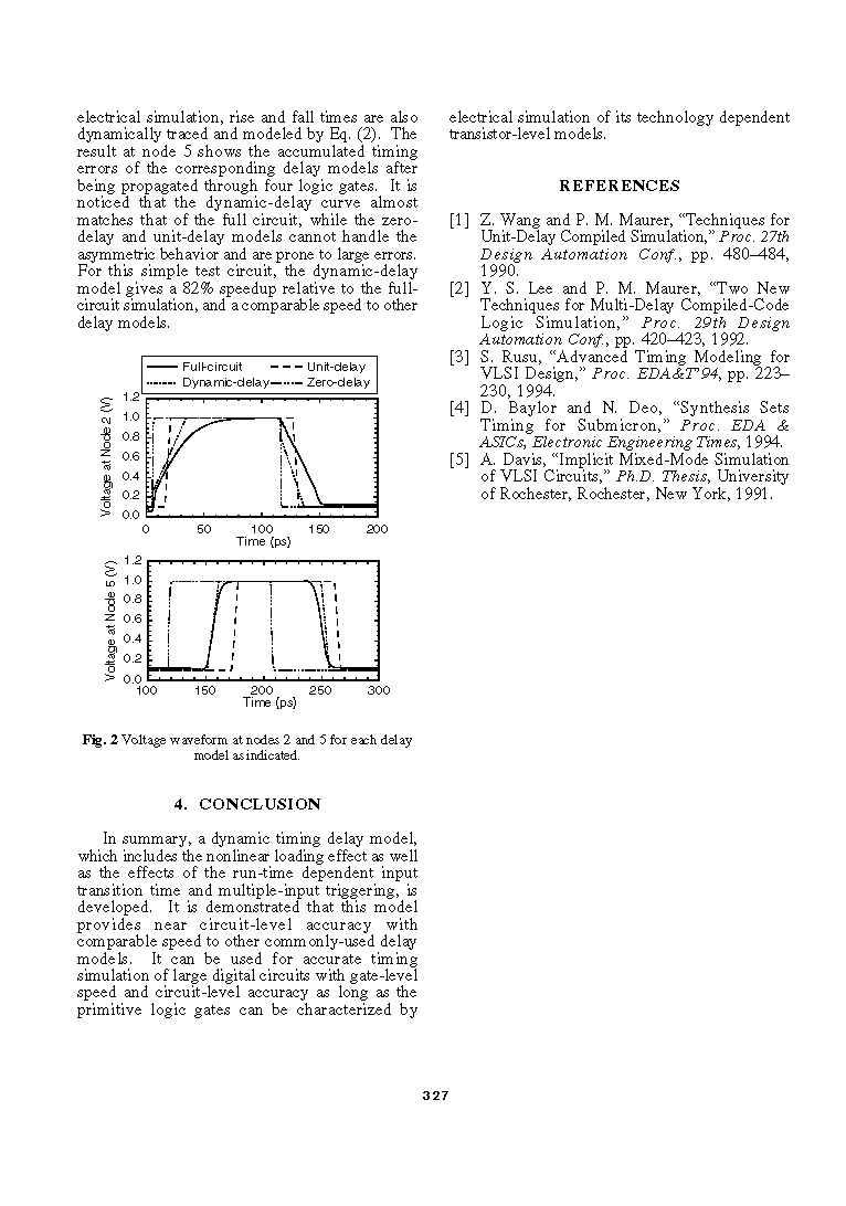
Fig. 2 Voltage waveform at nodes 2 and 5 for each delay model
as indicated.