Facilities in SpinLab
Sample and Device Fabrication
AJA1800 Sputtering tool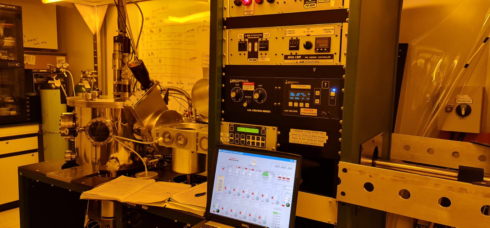
6 targets, DC magnetron, RF sputtering and RF etching
A thin film stack containing 5 metallic layers and 1 insulating layers can be deposited
Back
Back
Back
Back
Back
Back
Back
Back
Back
Back
Back
Back
AJA2200 Sputtering tool
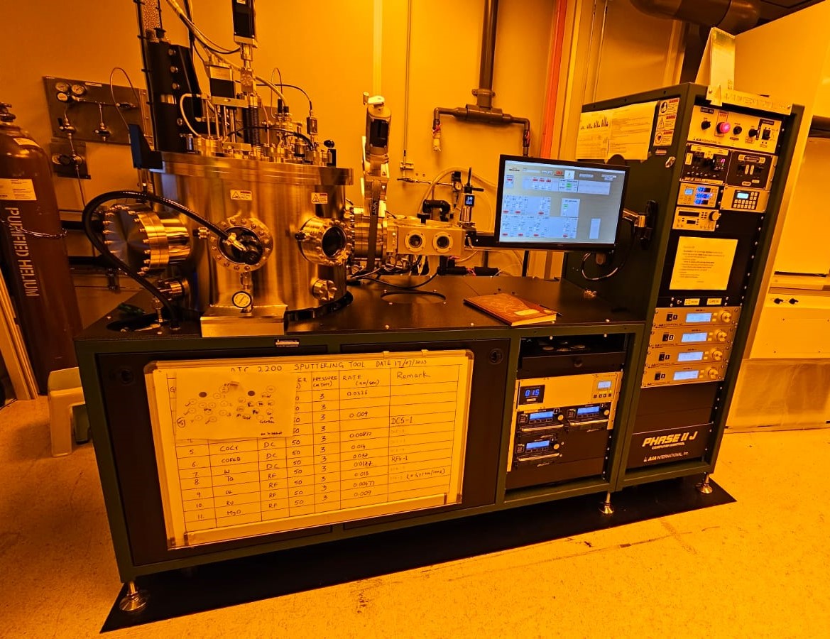
12 targets, DC magnetron and RF sputtering, co-sputtering for composition tuning
AJA Ion Milling tool
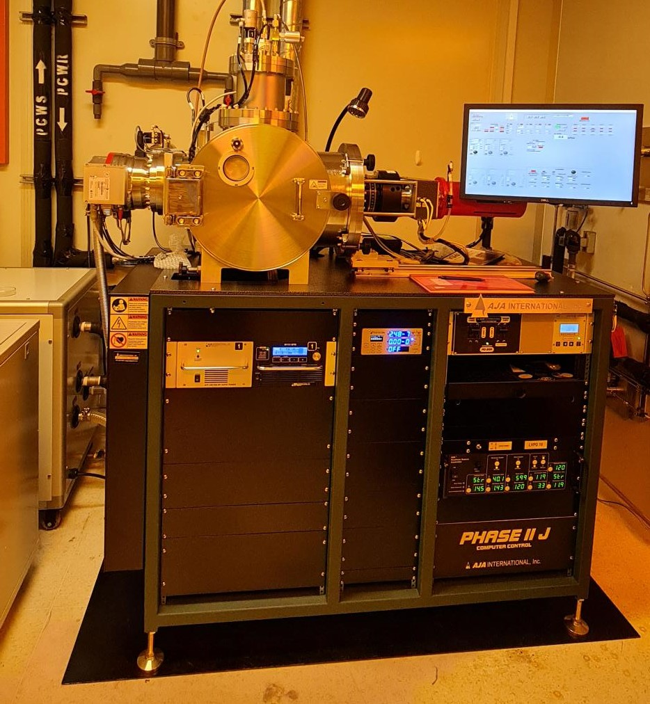
Ion milling tool with 1 sputter gun for SiO2 coating
MicroWriter ML3 model Maskless lithography
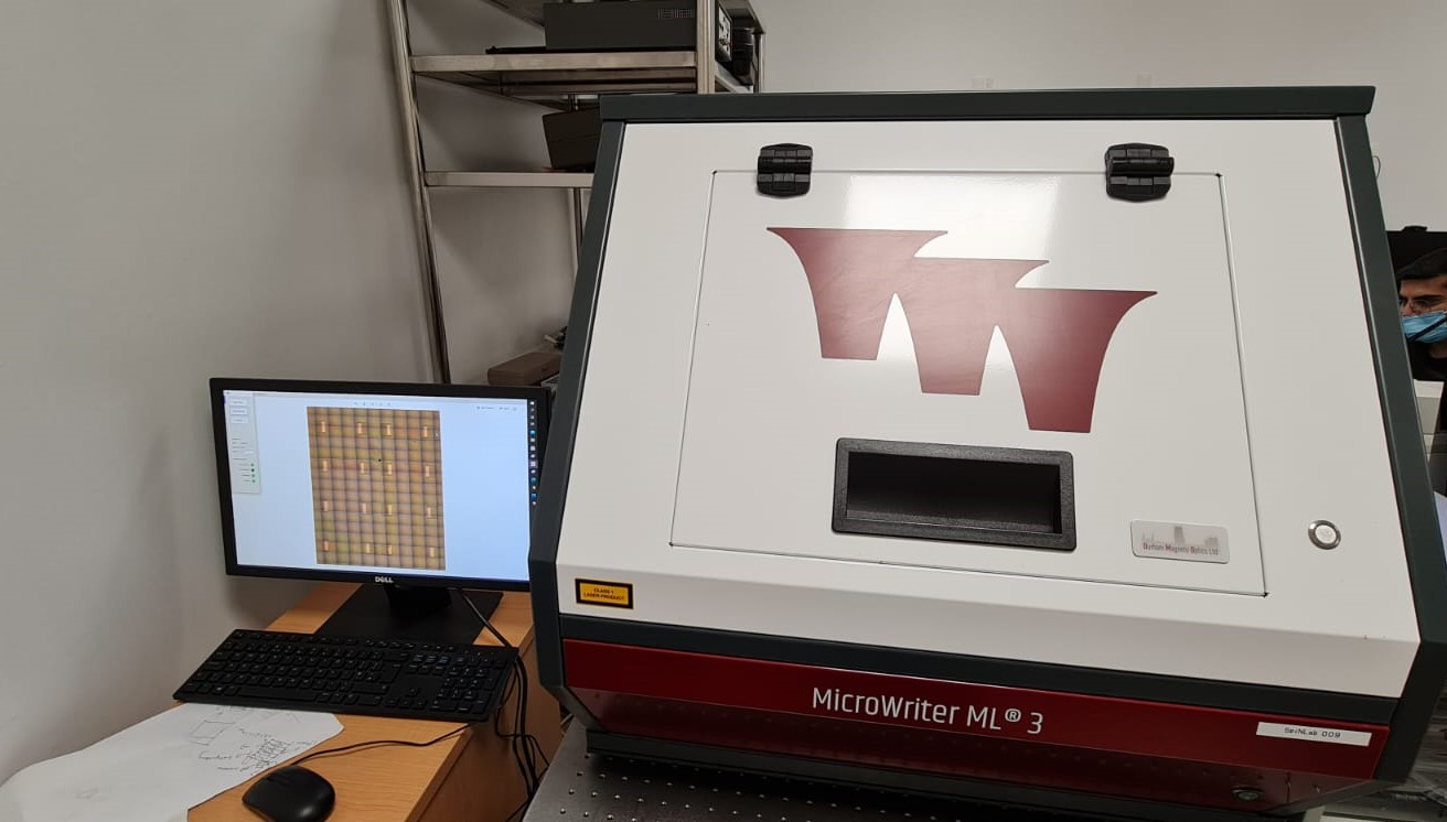
Maskless lithography, 1.5um resolution
Custom patterns can be drawn using PAINT or KLayout and lithography can be carried out without masks
NanoFrazor lithography
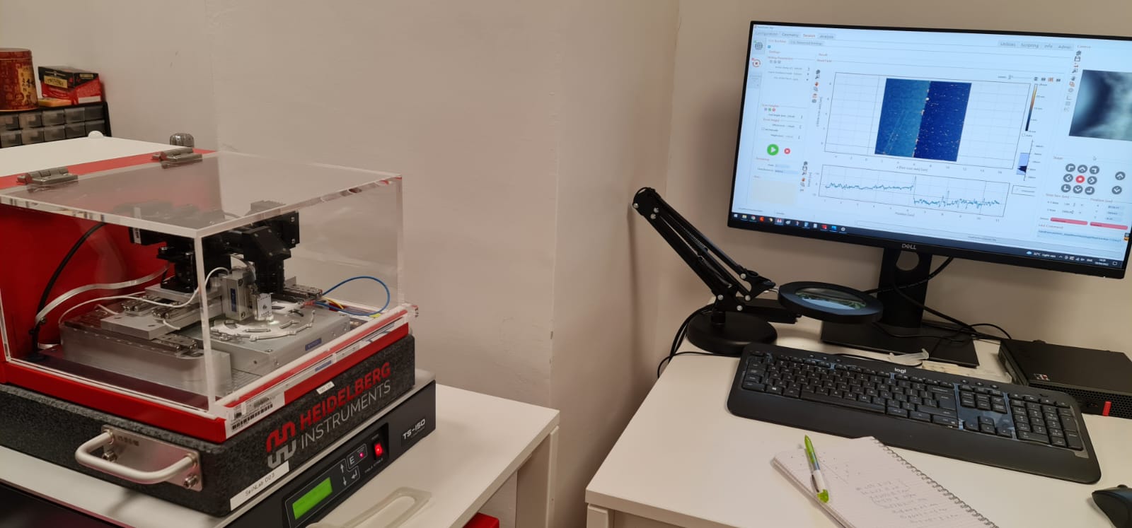
Mask less lithography for nanostructures, 30 nm resolution
NILT Nanoimprint lithography
Imprint lithography, sub-100 nm resolution
Lithography on 4" substrates can be carried out at high throughputs, for mass fabrication of patterns.
Wetbench (spin coater, ultrasonic cleaner, hotplate etc.)
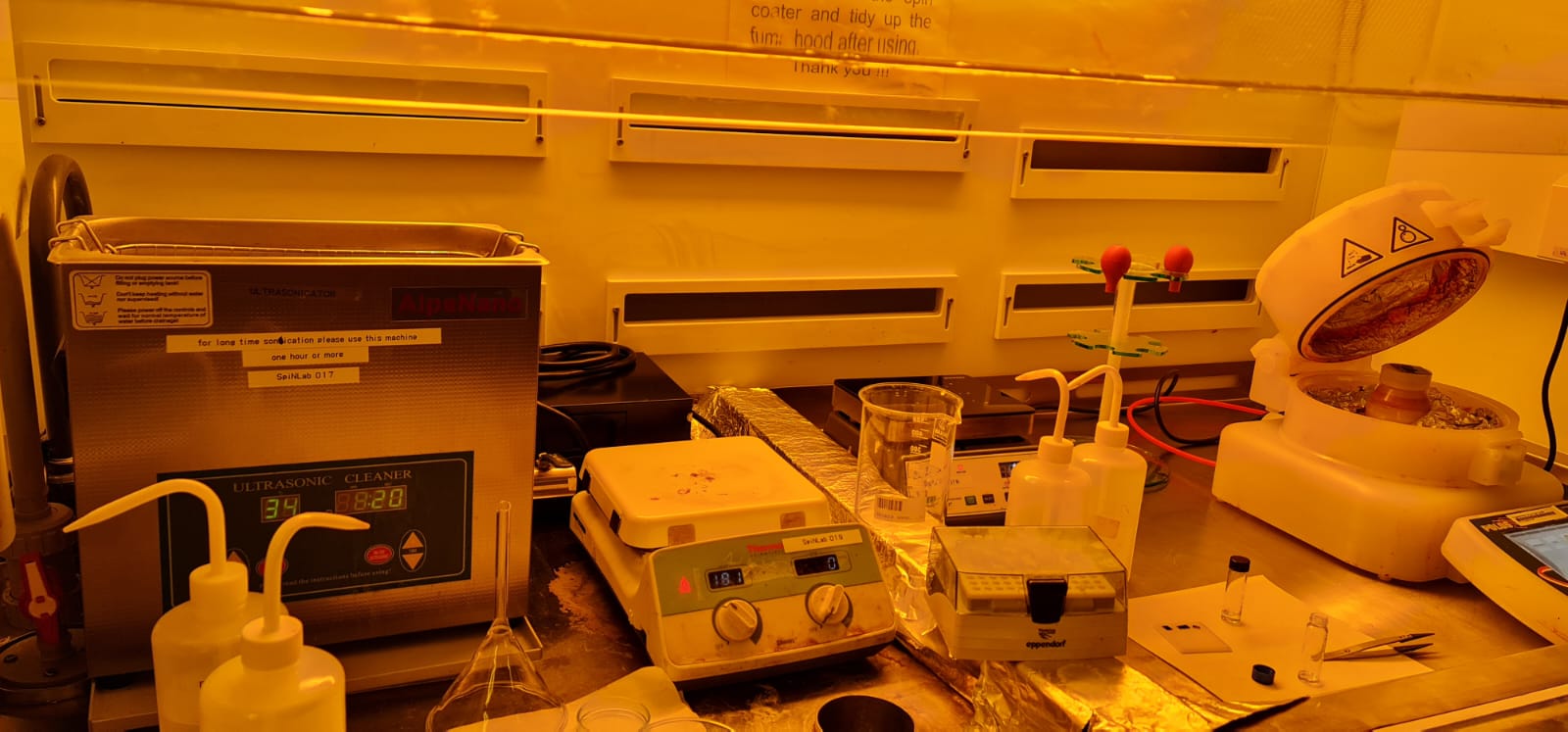
Spin coater, ultrasonic cleaner, hotplate etc.
Wirebonder
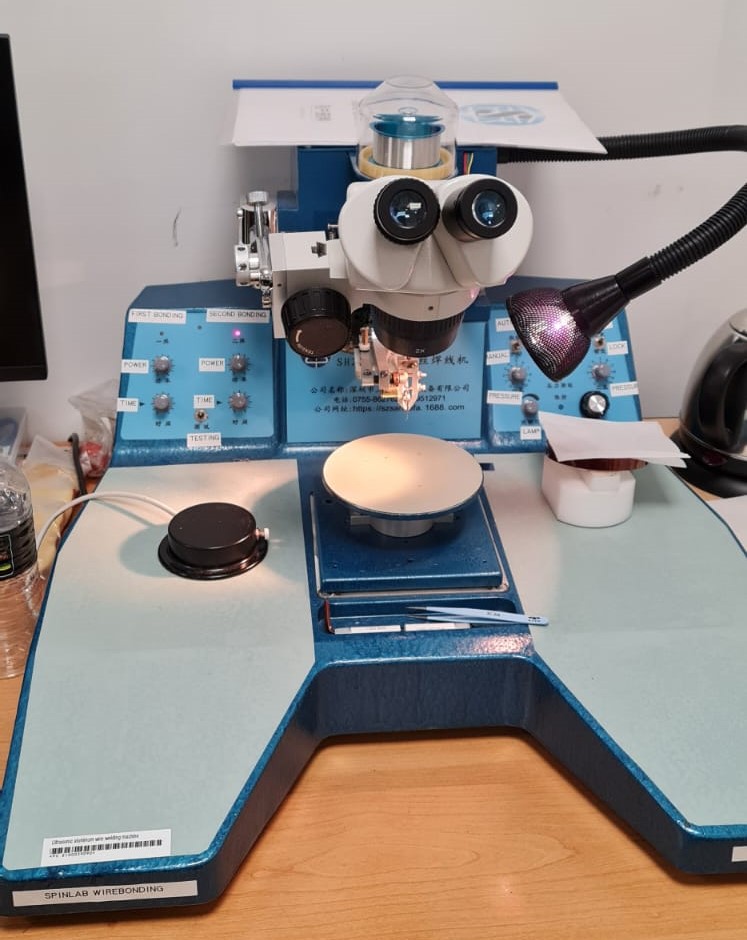
Wirebonders for electrical connections
Characterization tools
Electromagnet
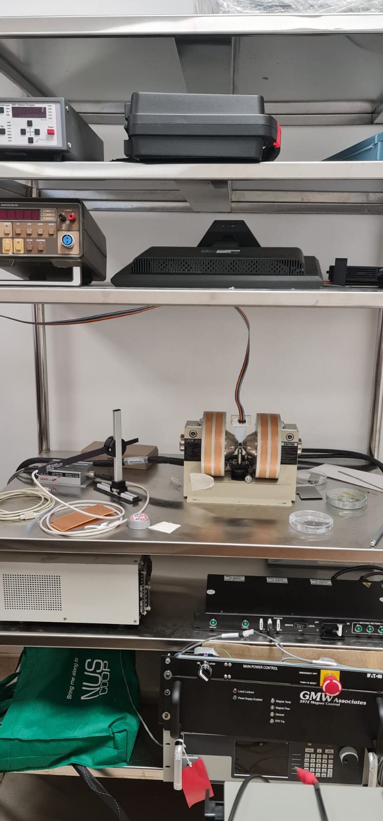
Electromagnet with 1.5-2 T magnetic field for various measurements
Electrical device measurements
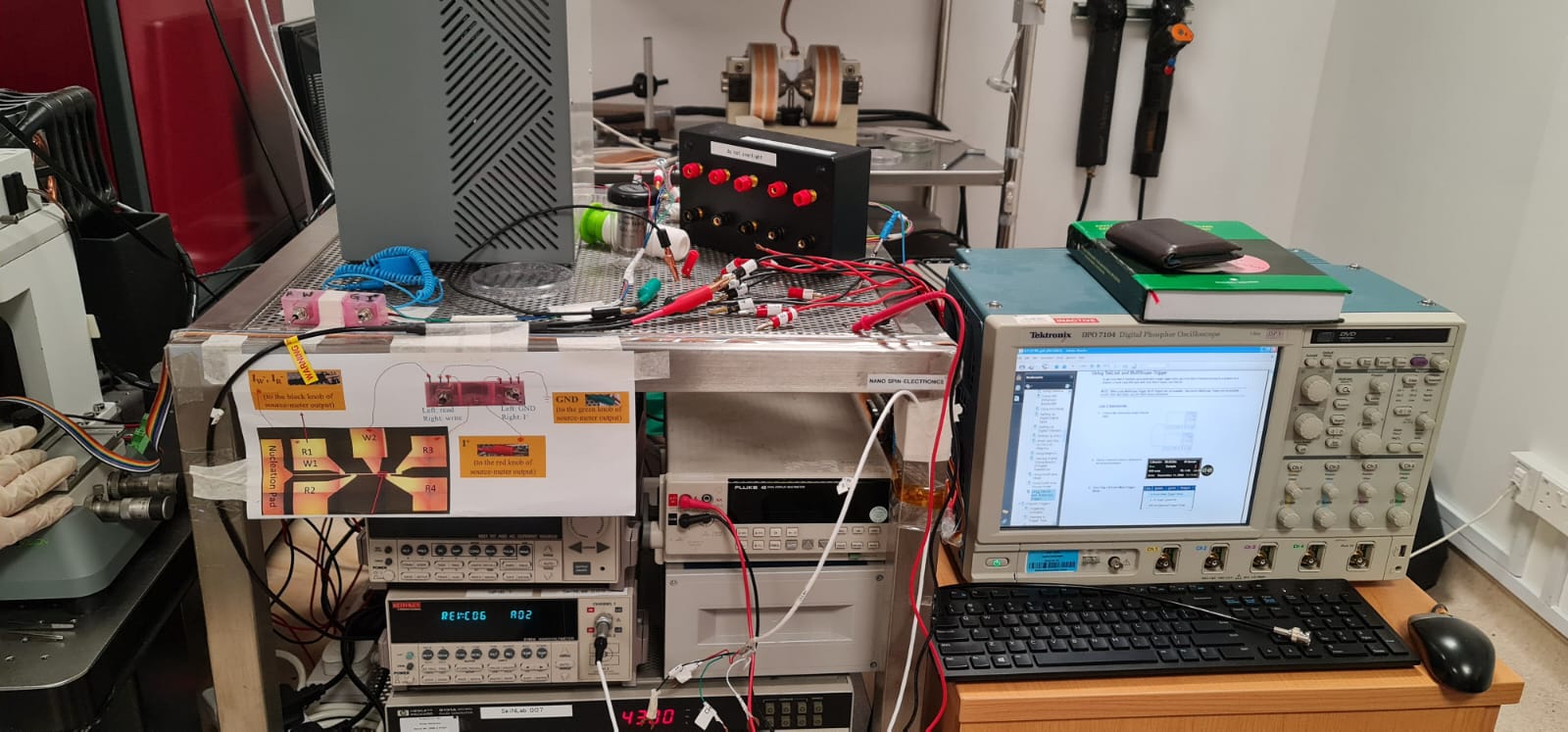
Electrical measurements (in the presence of a magnet) using Keithley voltage and current sources etc.
MagVision Kerr Microscopy
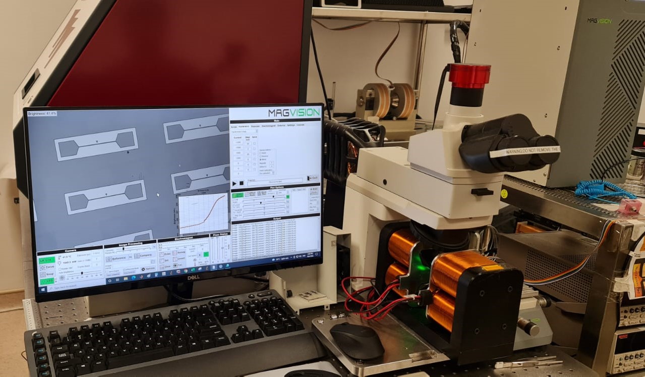
Kerr Microscopy / hysteresis loops in magnetic fields of about 1T in vertical directiion, 0.5 T any direction
Back
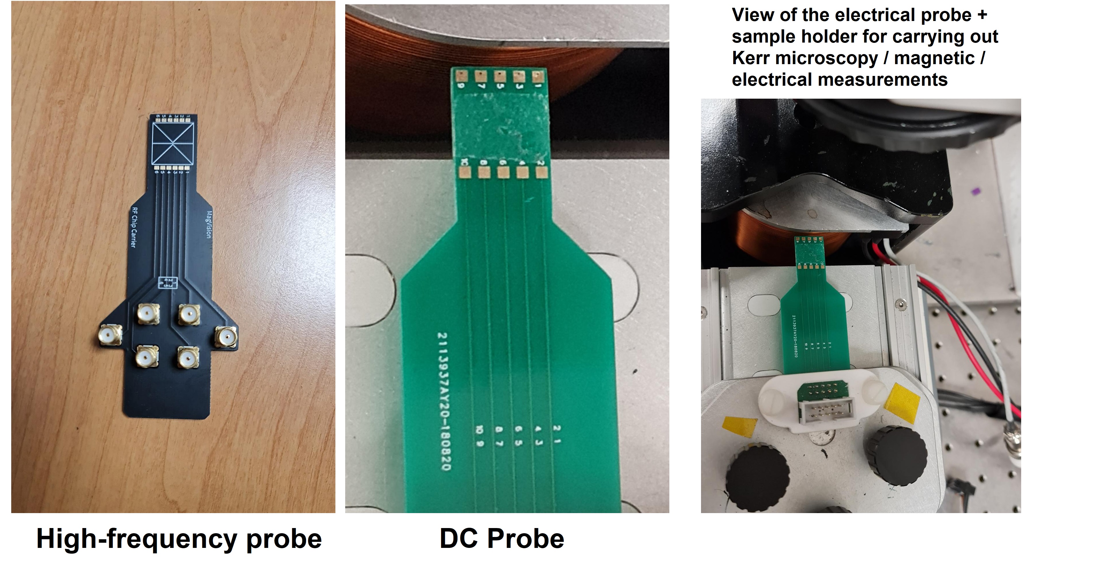
Electrical probes for Kerr Microscopy system
Back
Domain wall propagation in a magnetic material with a perpendicular magnetic anisotropy, observed using Kerr Microscopy. If black implies north poles up, grey implies south poles up
Atomic Force Microscopy
Atomic force microscopy can be measured using NanoFrazor tool
Workstations for simulations
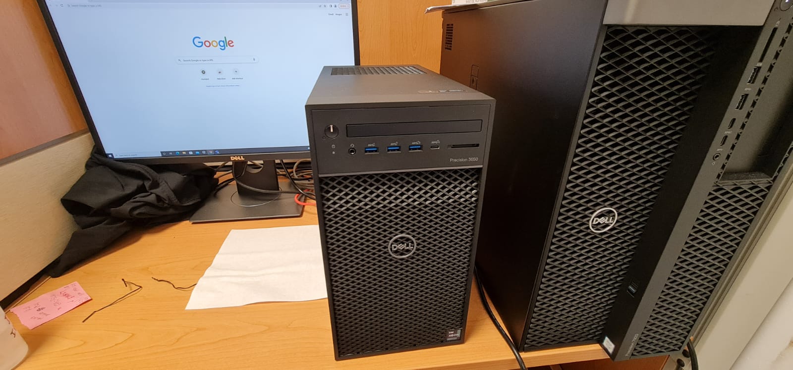
Workstations with GPUs for micromagnetic simulations
Common facilities
Various common facilities such as MFM/VSM/XRD etc. are available