Fusion Double Tilt TEM holder
For high-resolution, high temperature and/or biasing TEM experiments
Poseidon Select TEM holder
For electrochemistry in a liquid environment TEM experiments
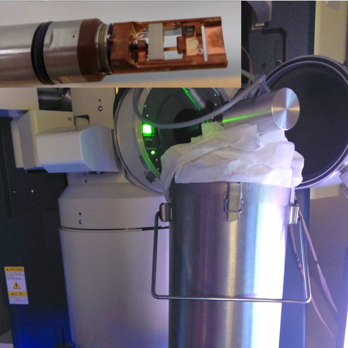
MEMS-based 6 Contacts Double Tilt Cooling holder
Able of 1A resolution from 120 K to 1000 K
Complex metallic alloy specimen on MEMS chip
FIB milling and in situ lift-out for the preparation of high-quality AlMnFe complex metallic alloy specimens for in situ annealing experiments in the TEM.
The electron-transparent area is prepared after the lamella has been transfered to the MEMS chip.
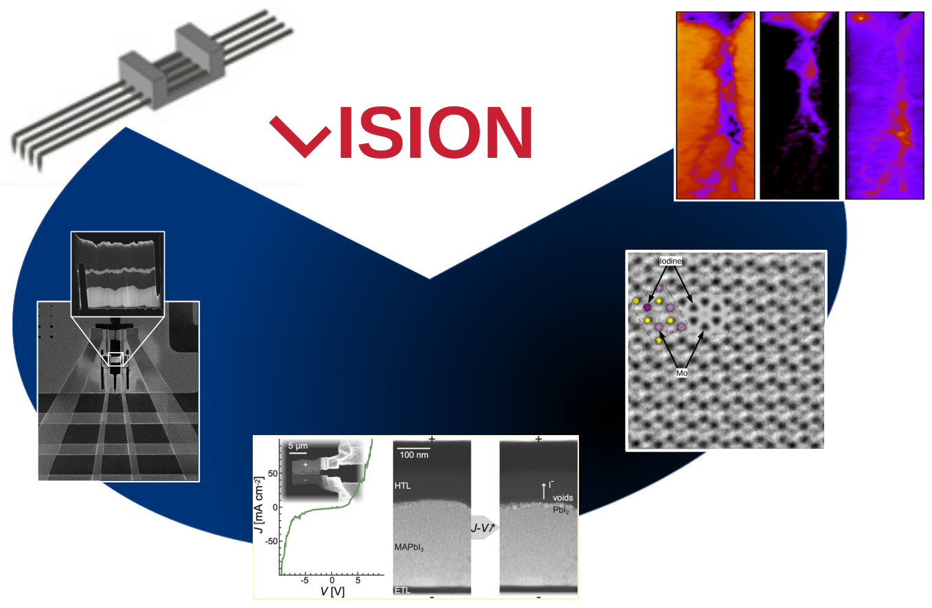
Electrically contacted Si solar cell on a MEMS chip
FIB milling and in situ lift-out for the preparation of high-quality specimens for in situ biasing experiments in the TEM.
The electron-transparent lamella is prepared after the lamella has been transfered to the MEMS chip.
Perovskite Solar Cells under Electrical Bias
HAADF-STEM images recorded when biasing at different current densities an organic/inorganic metal-halide perovskite solar cell
Resistive Switching in thin Silicon Oxide layer
In operando observation of the formation of a conductive path in the SiOx layer recorded while applying a bias locally to the specimen in the TEM
High-quality InN
Dislocations over the InN/GaN interface
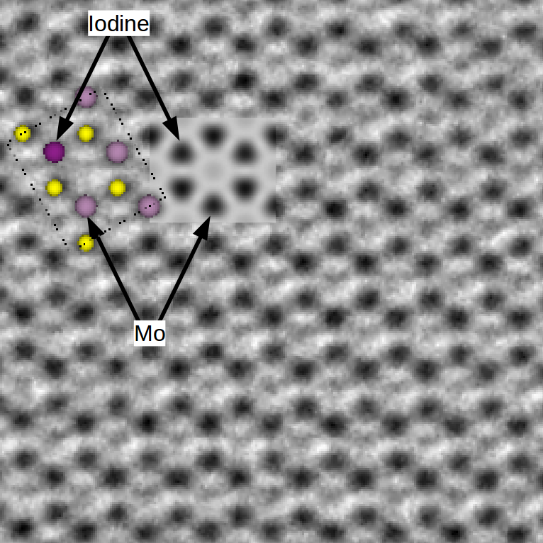
I-doped MoS2
80 kV Cs and Cc-corrected image (FEI Pico) overlaid with multi-slice image simulation (Dr Probe) and crystal structure
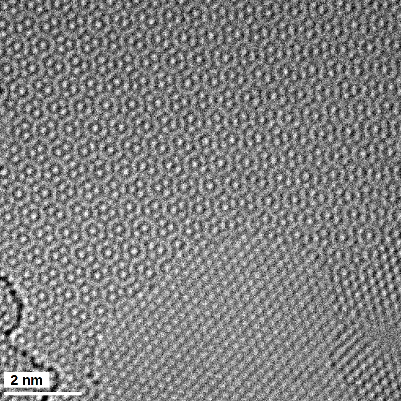
Mono and Bi-layers Graphene
80 kV Cs and Cc-corrected image (FEI Pico) taken at 300°C using wildfire TEM holder
Defective area in μc-Si:H solar cell
Spectral components obtained by decomposing an EEL spectrum dataset using VCA algorithm
CoFe2O4/BaTiO3 interface
EEL spectra of the Ti L3,2, O K, Fe L3,2, Co L3,2, and Ba M5,4 edges and the corresponding ADF
image across the interface
Nanometer STEM-EELS plasmon mapping
Spatially resolved mapping of surface plasmon resonances by EELS and BEM simulations of hollow cuboid metal nanostructures
