
Current research interests of Tze-Chien Sum and his group are on investigating light matter interactions; energy and charge transfer mechanisms; and probing carrier and quasi-particle dynamics in a broad range of emergent nanoscale and light harvesting systems using Femtosecond time-resolved spectroscopy. Within these seemingly broad material systems – organic and inorganic semiconductors, I address the following three questions: (1) Where did the energy go? That is the interplay of carrier/quasi-particle dynamics between the host energy levels, defect energy levels and the dopant energy levels. (2) What is the underlying photo-physics and light-matter interactions that gives this system its unique characteristics? That is the various processes such as carrier-carrier scattering, carrier-phonon scattering, radiative recombination and auger recombination etc. (3) How can these properties/technologies be harnessed for practical applications? That is how the knowledge gained be used for the development of novel optoelectronic devices with enhanced efficiency and sensors with better sensitivity.
Broadly, I can categorize my group’s efforts in three main areas: (A) nanomaterials nanophotonics; (B) mixed dimension heterostructures; and (C) photovoltaics (PV) and plasmonic PV. Highlights from these works are showcased below:
The schematic depicts two semiconductor nanowires under lasing action with single photon excitation (SPE) vs two photon excitation (TPE). The commonly accepted paradigm that the higher pump intensities needed for two photon excitation (TPE) would correspond to higher exciton density threshold (nth) for two-photon pumped lasing is re-examined by Tze-Chien Sum and co-workers using femtosecond time-resolved spectroscopy. Our results show that a much lower nth is needed to achieve lasing in single ZnSe nanowires with TPE compared to single photon excitation (SPE). This finding has significant implications for the photo-stability and durability of nanowire lasing.
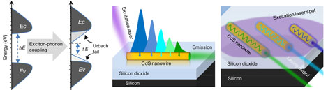
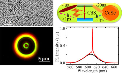
Another recent featured work is on the development of a new approach for tailoring the nanowire lasing modes in CdS nanowires. This method is based on the intrinsic self-absorption of the gain media (via the Urbach tail states) to achieve low-loss, room-temperature NW lasing with a high degree of mode selectivity (over 30 nm). Importantly, this straight-forward approach is widely applicable in most semiconductor or semiconductor/plasmonic NW cavities.
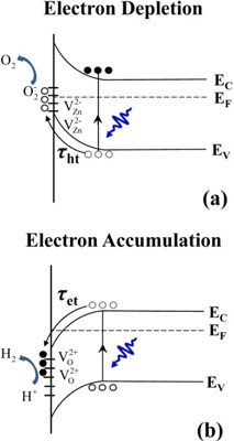
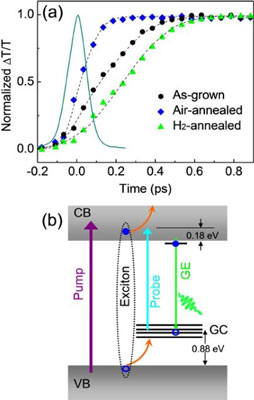
The defect related green emission has often been "blamed" for the quenching of the ZnO band edge emission. However, our findings revealed an ultrafast hole-transfer process to the surface adsorbed oxygen species (e.g., O2-) occurring within a few hundred picoseconds (ps) in the air-annealed samples; and an ultrafast electron-transfer process to charged oxygen vacancies (i.e., VO2+) occurring within tens of ps in the H2-annealed samples – see Fig.
Contrary to the common perception that the bandedge emission (BE) dynamics are strongly influenced by the carrier trapping to the green emission related defect states, these above processes compete very effectively with the ZnO BE. Hole trapping by VZnO, which occurs in an ultrashort sub-ps-to-ps timescale (and hence limits its effective hole capture radius), however, has less influence on the BE dynamics. Importantly, our findings shed new light on the photoinduced charge transfer processes that underpins the novel properties of enhanced photocatalytic activity, photovoltaic performance, and photoconductivity response of ZnO NWs; thereby suggesting a strategy for tailoring the ultrafast carrier dynamics in ZnO NW-based devices.
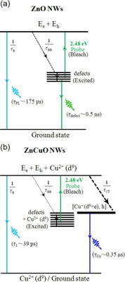
Copper is one of the most pervasive and important impurities in ZnO. Over the past four decades, there have been extensive studies on this CuZn defect which manifest itself as the green luminescence (GL) band peaking at ~2.45eV. At low temperatures, the GL exhibits a distinct phonon-related fine structure and a zero-phonon line at ~2.86 eV. The origin of this GL band is attributed to the [Cu+ (d9 + e), h] → [Cu2+ (d9)] + hv charge transfer transitions where the hole is transferred from a level highly perturbed by the surrounding oxygen to the highly shielded d shell of the copper atom. In this intermediately bound exciton model, the electron wavefunction of the tenth electron in the Cu+ ion is delocalized due to the hybridization of the d states with the bottom of the conduction band, thus being depicted as: [Cu+ (d9 + e), h].
In this work, we present the first experimental evidence of this ultrafast CT process between the ZnO host and the Cu dopants following above-bandgap photoexcitation. An electron capture lifetime of 39 ± 9 ps by Cu2+ (d9) was measured.
The origin and the mechanism of the green defect emission in ZnO nanowires is another long standing controversy in the ZnO field. In our earlier work published in PCCP, we had focused on the separating the competing recombination pathways due to the surface state of the nanowires. In this work, we established that the fast trapping of carriers to the green-emission related centers is through an ultrafast excitonic Auger recombination mechanism. We found that the green emission originates from the recombination between the electrons in the conduction band and/or shallow donor levels and the holes trapped at the green emission centers (believed to be VZnO di-vancancies).
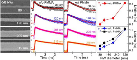
Size, surface trapping, and scattering effects have a pronounced influence on the recombination dynamics nanowires (NWs). It is often very difficult to differentiate these intertwined effects. Herein, we present a comprehensive study on the size-dependent exciton recombination dynamics of high quality CdS NWs (with diameters from 80 to 315 nm) using temperature-dependent and time-resolved photoluminescence (TRPL) spectroscopy in a bid to distinguish the contributions of size and surface effects. Our findings discerned the interplay between size and surface effects and advanced the understanding of size dependent optoelectronic properties of one-dimensional semiconductor nanostructures for applications in surface- and size related nanoscale devices.
Utilizing the CdS shell as an antenna for light harvesting and the quantum confinement afforded by the size of the dot, our group has been able to achieve ultralow threshold lasing over a range of emission wavelengths. This ultralow threshold is achieved through the large absorption cross-sections and suppressed Auger recombination rates in these nano-heterostructures. This work is published in ACSNano (2012).
Using the same concept, ultralow threshold lasing was also realized in tetrapods. This work is published in Advanced Materials.
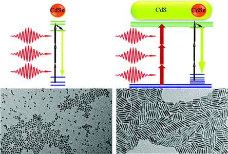
In these works, we presented a strategy that permits the independent tuning of the MPA cross-section and the luminescence properties using semiconductor core/enlarged-shell QDs. We demonstrate this with a representative CdSe/CdS nanodot/nanorod system. The elongated CdS shell is used as a photon-capturing "antenna", which can greatly enhance the overall MPA cross-section of the QD. 2PA and 3PA cross-sections 2-3 orders larger compared to CdSe/CdS QDs can be achieved using these seeded CdSe/CdS nanorod heterostructures. Furthermore, we also proposed a simple model accounting for the effective 3PA absorption cross-sections for various II-VI semiconductor quantum dots obtained with different lasers pulse widths. Importantly, this unifying picture provides users with a clear basis of comparison for the 3PA cross-sections obtained with different laser pulse widths for various II-VI semiconductor quantum dots. This will facilitate users to make a more judicious choice for their use in MPA applications.
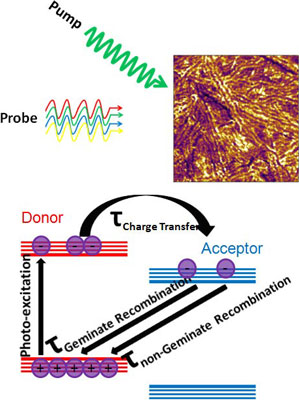
Organic photovoltaic (OPV) devices fabricated with P3HT nanofiber (NF) networks typically exhibit poorer device performance compared to their nanoscale phase separated P3HT:PCBM counterparts despite possessing superior light harvesting properties and high in-plane charge mobility. Herein, we investigate the charge generation and recombination dynamics in P3HT-NF:PCBM blend films using transient absorption spectroscopy (TAS) spanning a wide temporal range over 7 orders of magnitude (i.e., from 100 fs to 1 μs), which are correlated with device performance studies. TAS reveals a more efficient charge generation and polaron formation rate in the NF samples as compared to the control samples at the onset which persists up to ∼2 ns. However, within the nanoseconds to microseconds time scale, there is a significant amount of nongeminate recombination in the NF system. We attribute this to the poor interfibrillar charge transport between the NFs, which tend to align parallel to the electrodes, thereby causing charge localization. These charge dynamics were validated using the analytical model proposed by Laquai and co-workers [Howard, I. A.; et al. J. Am. Chem. Soc. 2010, 132, 14866]. Importantly, our findings provide new insights into the factors that limit the photovoltaic performance of such P3HT-NF based devices.
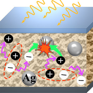
Recently, a team of researchers from Nanyang Technological University (NTU) led by Associate Professor Sum Tze-Chien uncovered a significant loss mechanism in silver nanoparticle blended bulk heterojunction (BHJ) plasmonic organic solar cells (OSCs) using ultrafast optical spectroscopy. Metal nanoparticles (NPs) are commonly used to facilitate light trapping in plasmonic OSCs, but they can also reduce cell performance. Presently, there is a controversy over the positive and negative influence of adding metal NPs to BHJ OSCs. Ultrafast optical spectroscopy provides unambiguous evidence that a trap-assisted recombination of charge carriers by the NPs leads to degradation, irrespective of an initial enhanced absorption and excitation. Our findings, correlated with electrical device characterization, provide new insights into the fundamental photophysics and charge dynamics in plasmonic OSCs. Importantly, our work would resolve the present controversy in the field. This work was published online in Nature Communications on 13 June 2013.
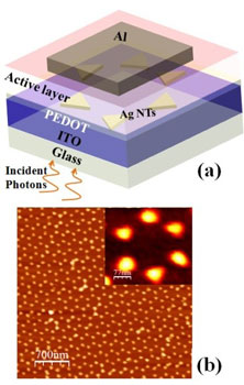
In this work, we demonstrated efficiency enhancement in plasmonic bulk heterojunction (PCDTBT:PCBM) organic solar cells (OSCs) integrated with large-area periodic Ag nanotriangle (NT) arrays in the OSC device. These Ag NT arrays were fabricated using the cost-effective, high-throughput nanosphere lithography technique. The improvements to the power conversion efficiency (from 4.24 to 4.52%) and to the short circuit current density (by ∼12%) are attributed to an increase in exciton generation induced by the strong local E-field and the scattering generated by the localized surface plasmon resonance of the hexagonal NT arrays. These findings are validated by a range of steady-state and transient optical spectroscopy and correlated with device performance data. Importantly, our work demonstrates the feasibility of integrating a simple cost-effective, tailorable, and scalable nanofabrication technique with existing OSC fabrication processes.
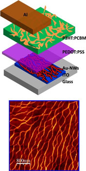
Solution-processed ultrafine gold nanowires (Au-NWs) have been exploited as plasmonic antennae in organic P3HT:PCBM photovoltaic cells. The careful reduction of the spacer layer thickness which allows the evanescent field to be extended into the photoactive layer and the geometry of the Au-NWs bands which favors the enhanced scattering collectively result in an increased short-circuit current density by 23.2%. The exact nature of the plasmonic effect in Au-NWs incorporated P3HT system and the critical role played by the spacer layer were studied through optical and time-resolved photoluminescence spectroscopy. The improved photocurrent in the Au-NWs integrated devices is due to an enhanced absorption in the photoactive layer which is contributed from an increased plasmon excitation field and far-field scattering of Au-NWs