Photovoltaics, LEDs, Scintillators with Perovskite materials
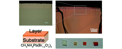
Large 3D Crystaline Perovskites
Double heterostructure on a large hybrid halide perovskite crystal
The solvothermal liquid-phase growth process with low halide composition gradient and solution concentrations just above the critical supersaturation, we have controlled halide ion interdiffusion.
Two consecutive layers are grown to create a double heterostructure for the first time with a large perovskite crystal.
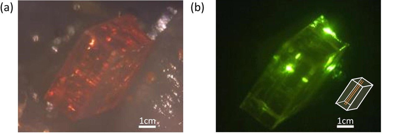
Room temperature electroluminescence from large perovskite single crystals
A simple fabrication method was used to obtain an active perovskite region between two gold wire electrodes. The perovskite is pristine single crystal, well isolated from surroundings through fabrication to the characterization process.
Current oscillations and intermittent emission are caused by ion-mediated negative differential resistance and conductive filament formation, respectively.
Strong Plasmon-Wannier Mott Exciton Interaction with High Aspect Ratio Colloidal Quantum Wells
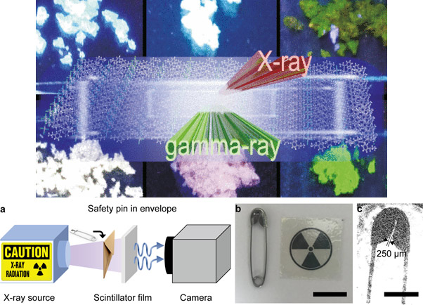
Organic/inorganic hybrid perovskite crystals, 2D and quantum dots are excellent scintillation materials.
Besides very good light yields (between 10,000 and 40,000 photons/MeV) very much similar to commercial materials, their response is very fast with few orders of magnitute compared to current scintillators in the market
With doping strategy, the materials promise versatile scintillators for X-ray, gamma-ray, and even thermal neutrons.
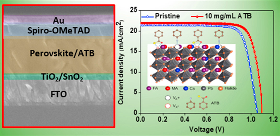
Engineering charge transport layers to enhance perovskite photovoltaics' performance
Various strategies are employed to engineer the electron and hole transport layers such as: binary/ternary metal oxides, interfacial engineering, doping /co-doping.
The engineered charge transport layers enhance photovoltaic device performance by improving the energy band alignment, reducing the traps, increase the stability.